- 您现在的位置:买卖IC网 > Sheet目录336 > IXDN414YI (IXYS)IC DRIVER MOSF/IGBT 14A 5-TO-263
IXDN414PI / N414CI / N414YI / N414SI
IXDI414PI / I414CI / I414YI / I414SI
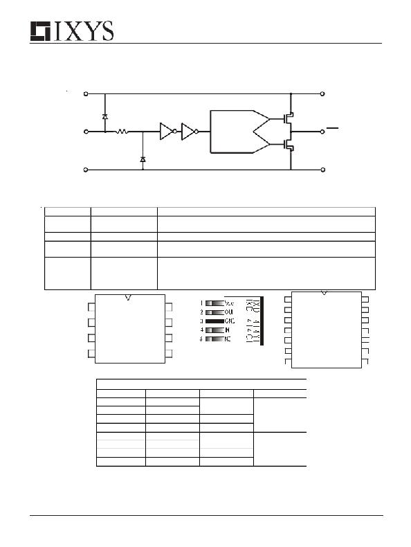
Figure 2 - IXDI414 Inverting 14A Gate Driver Functional Block Diagram
Vcc
ANTI-CROSS
P
Vcc
IN
CONDUCTION
OUT
GND
Pin Description And Configuration
CIRCUIT *
N
GND
SYMBOL
VCC
IN
OUT
GND
FUNCTION
Supply Voltage
Input
Output
Ground
DESCRIPTION
Positive power-supply voltage input. This pin provides power to the
entire chip. The range for this voltage is from 4.5V to 35V.
Input signal-TTL or CMOS compatible.
Driver Output. For application purposes, this pin is connected via an
external resistor to a Gate of a MOSFET/IGBT.
The system ground pin. Internally connected to all circuitry, this pin
provides ground reference for the entire chip. This pin should be
connected to a low noise analog ground plane for optimum
performance.
1 VCC
2 IN
3 NC
4 GND
I
X
D
(1)
4
1
4
P
I
VCC 8
OUT 7
OUT 6
GND 5
TO220 (CI)
TO263 (YI)
1 NC
2 NC
3 VCC
4 IN
5 NC
6 GND
7 NC
I
X
D
(1)
4
1
4
S
I
NC 14
NC 1 3
VCC 1 2
OUT 1 1
OUT 1 0
GND 9
NC 8
8 PIN DIP (PI)
ORDERING INFORMATION
14 PIN SOIC
Part Number
IXDN414PI
IXDN414SI
IXDN414CI
IXDN414YI
IXDI414PI
IXDI414SI
IXDI414CI
IXDI414YI
Package Type
8-Pin PDIP
14-Pin SOIC
5-Pin TO-220
5-Pin TO-263
8-Pin PDIP
14-Pin SOIC
5-Pin TO-220
5-Pin TO-263
Temp. Range
-55 ° C to 125 ° C
-55°C to 125°C
-55 ° C to 125 ° C
-55 ° C to 125 ° C
-55 ° C to 125 ° C
-55 ° C to 125 ° C
Configuration
Non Inverting
Inverting
NOTES 1: Either "I" or "N";
2: Mounting or solder tabs on all packages are connected to ground
* Patent Pending
2
发布紧急采购,3分钟左右您将得到回复。
相关PDF资料
IXDN509D1T/R
IC GATE DRIVER SGL 9A 6-DFN
IXDN514SIAT/R
IC GATE DRIVER SGL 14A 8-SOIC
IXDN602PI
MOSFET N-CH 2A DUAL LO SIDE 8-DI
IXDN630CI
IC GATE DRIVER LOW SIDE 5TO220
IXDS430SI
IC DRVR MOSF/IGBT 30A 28-SOIC
IXS839S1T/R
IC MOSFET DRIVER SYNC BUCK 8SOIC
JLINK-RX-AD
ADAPT BD FOR MINI-JTAG CONNECTOR
JMBADGE2008-B
BOARD JM BADGE
相关代理商/技术参数
IXDN414YM
制造商:IXYS 制造商全称:IXYS Corporation 功能描述:14 Ampere Low-Side Ultrafast MOSFET Drivers
IXDN430
制造商:IXYS 制造商全称:IXYS Corporation 功能描述:30 Amp Low-Side Ultrafast MOSFET / IGBT Driver
IXDN430CI
功能描述:功率驱动器IC 30 Amps 40V 0.4 Rds RoHS:否 制造商:Micrel 产品:MOSFET Gate Drivers 类型:Low Cost High or Low Side MOSFET Driver 上升时间: 下降时间: 电源电压-最大:30 V 电源电压-最小:2.75 V 电源电流: 最大功率耗散: 最大工作温度:+ 85 C 安装风格:SMD/SMT 封装 / 箱体:SOIC-8 封装:Tube
IXDN430MCI
功能描述:功率驱动器IC 30 Amps 40V 0.4 Rds RoHS:否 制造商:Micrel 产品:MOSFET Gate Drivers 类型:Low Cost High or Low Side MOSFET Driver 上升时间: 下降时间: 电源电压-最大:30 V 电源电压-最小:2.75 V 电源电流: 最大功率耗散: 最大工作温度:+ 85 C 安装风格:SMD/SMT 封装 / 箱体:SOIC-8 封装:Tube
IXDN430MYI
功能描述:功率驱动器IC 30 Amps 40V 0.4 Rds RoHS:否 制造商:Micrel 产品:MOSFET Gate Drivers 类型:Low Cost High or Low Side MOSFET Driver 上升时间: 下降时间: 电源电压-最大:30 V 电源电压-最小:2.75 V 电源电流: 最大功率耗散: 最大工作温度:+ 85 C 安装风格:SMD/SMT 封装 / 箱体:SOIC-8 封装:Tube
IXDN430YI
功能描述:功率驱动器IC 30 Amps 40V 0.4 Rds RoHS:否 制造商:Micrel 产品:MOSFET Gate Drivers 类型:Low Cost High or Low Side MOSFET Driver 上升时间: 下降时间: 电源电压-最大:30 V 电源电压-最小:2.75 V 电源电流: 最大功率耗散: 最大工作温度:+ 85 C 安装风格:SMD/SMT 封装 / 箱体:SOIC-8 封装:Tube
IXDN502D1
功能描述:功率驱动器IC 2 Amps 35V 3 Rds RoHS:否 制造商:Micrel 产品:MOSFET Gate Drivers 类型:Low Cost High or Low Side MOSFET Driver 上升时间: 下降时间: 电源电压-最大:30 V 电源电压-最小:2.75 V 电源电流: 最大功率耗散: 最大工作温度:+ 85 C 安装风格:SMD/SMT 封装 / 箱体:SOIC-8 封装:Tube
IXDN502D1T/R
功能描述:功率驱动器IC 40V 4A RoHS:否 制造商:Micrel 产品:MOSFET Gate Drivers 类型:Low Cost High or Low Side MOSFET Driver 上升时间: 下降时间: 电源电压-最大:30 V 电源电压-最小:2.75 V 电源电流: 最大功率耗散: 最大工作温度:+ 85 C 安装风格:SMD/SMT 封装 / 箱体:SOIC-8 封装:Tube
